Crystal Overview
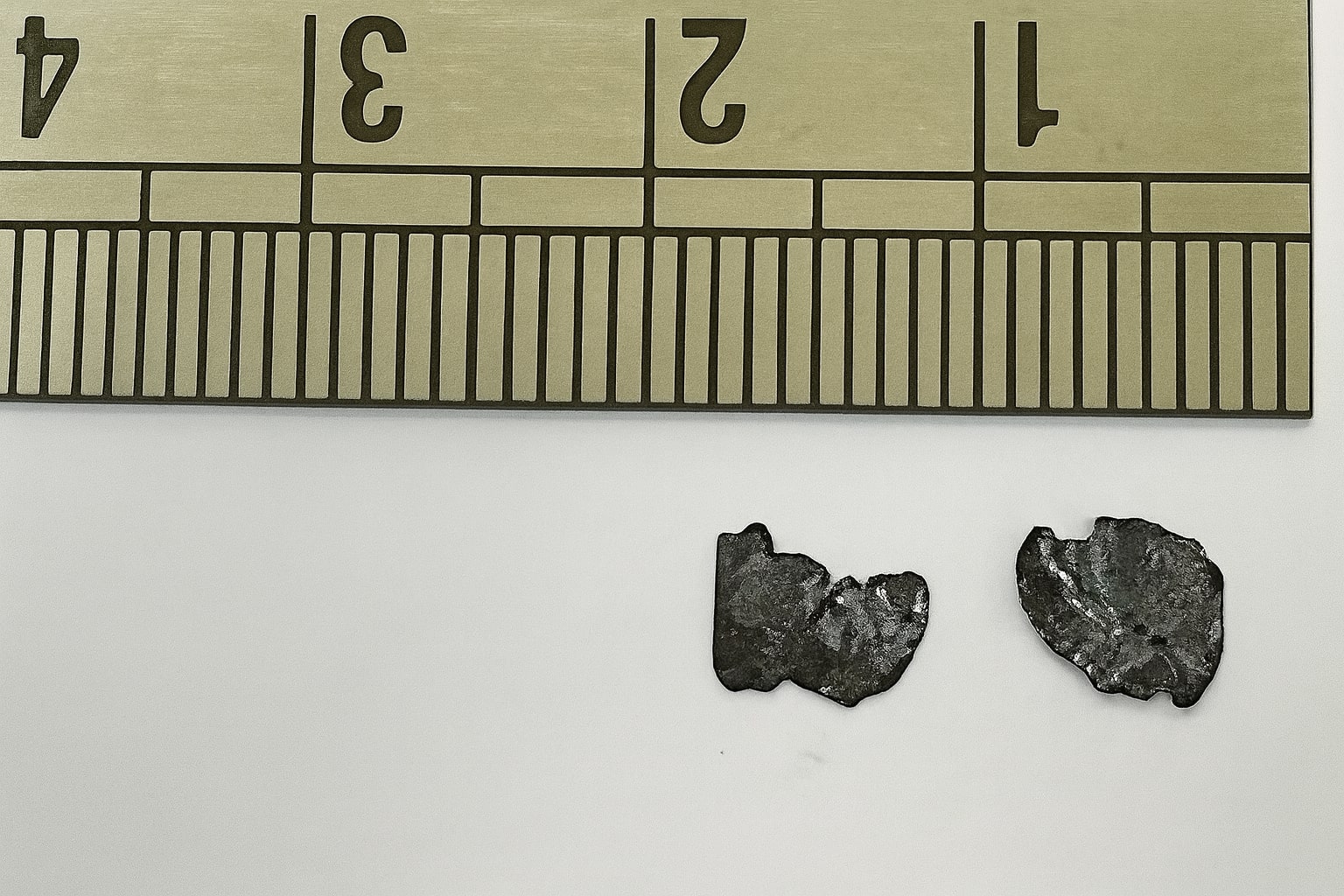
We supply large-area, high-purity indium selenide (In₂Se₃) single crystals. These crystals exhibit superior structural and electronic quality and are delivered exfoliation-ready for immediate use in research and device fabrication.
The In₂Se₃ single crystals are synthesized using Direct vapor transport (DVT) techniques, with growth parameters carefully optimized to ensure precise control over crystal phase, stoichiometry, and defect density. Post-growth refinement and annealing procedures further enhance structural order and phase purity.
Our crystals exhibit the following key properties:
- High crystallinity and phase purity: Verified by X-ray diffraction (XRD) and 4-angle rocking curve measurements, confirming (002) preferred orientation and excellent in-plane alignment of layered sheets.
- Exfoliation-ready layered structure: The material cleaves cleanly into thin flakes with atomically smooth surfaces, suitable for two-dimensional materials research.
- Well-defined electronic structure: Bulk crystals display a direct band gap of ~1.1-1.6 eV, making them highly suitable for optoelectronic, photonic, and semiconductor applications.
- Controlled phase composition: Unlike many commercially available In₂Se₃ materials, our synthesis protocol allows precise phase control, resulting in reproducible electronic and optical characteristics.
With their exceptional size, crystallinity, and electronic properties, these In₂Se₃ crystals provide an ideal platform for fundamental studies and high-performance device development.
Purchase