Crystal Overview
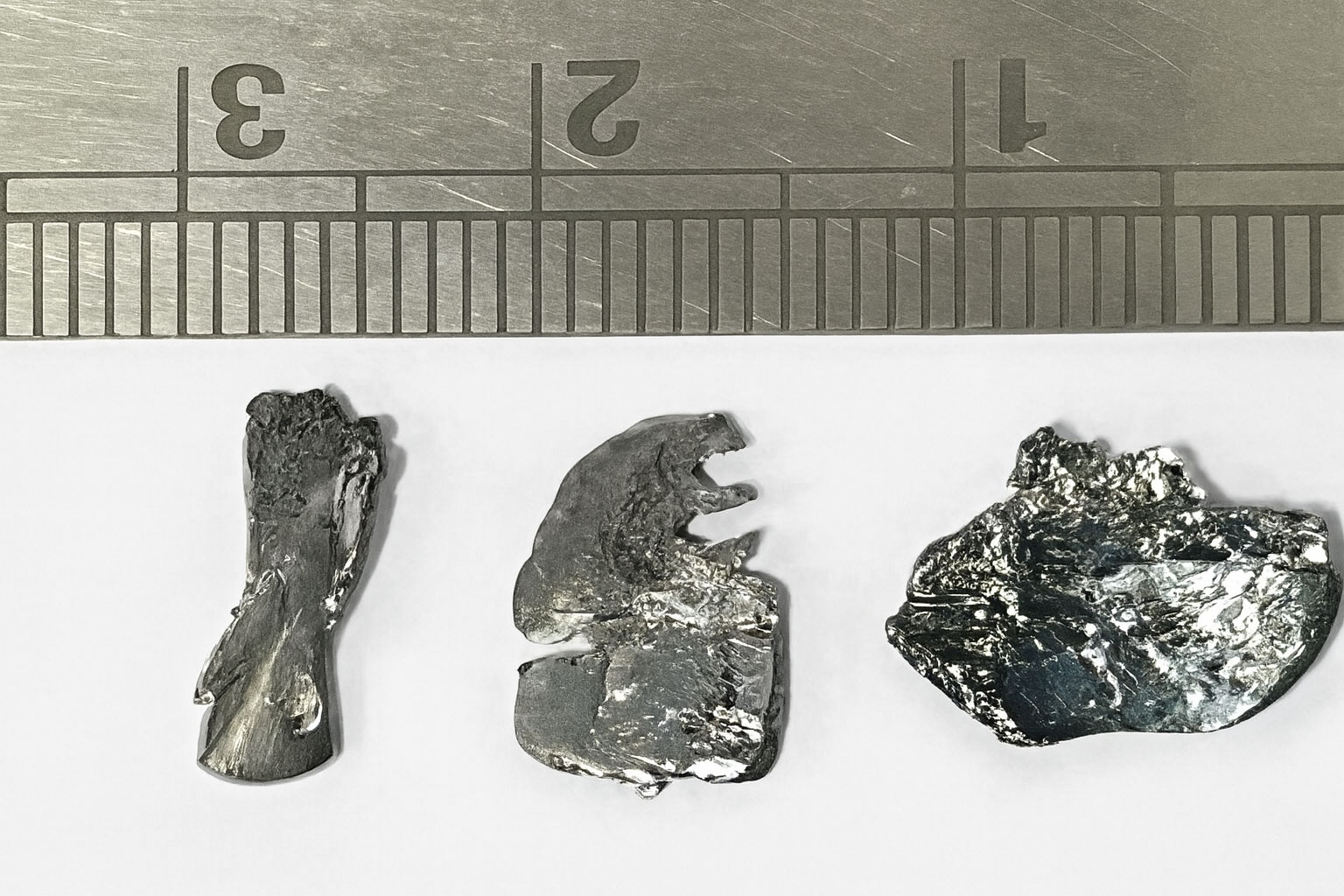
We supply large-area, high-purity tin selenide (SnSe) single crystals. These crystals exhibit excellent structural and electronic quality and are delivered exfoliation-ready for immediate use in research and device fabrication.
The SnSe single crystals are synthesized using Direct Vapor Transport (DVT) techniques, with growth parameters carefully optimized to control crystal orientation, stoichiometry, and defect density. Post-growth annealing and refinement procedures further improve structural order and phase purity.
Our crystals exhibit the following key properties:
- High crystallinity and phase purity: Verified by X-ray diffraction (XRD) and 4-angle rocking curve measurements, confirming (002) preferred orientation and excellent in-plane alignment of layered sheets.
- Exfoliation-ready layered structure: SnSe crystals cleave easily into thin flakes with atomically smooth surfaces, suitable for two-dimensional material studies and device integration.
- Well-defined electronic structure: Bulk crystals display a direct band gap of ~0.9-1.3 eV, making them suitable for thermoelectric, photonic, and electronic device applications.
- Controlled phase composition: Unlike many commercially available SnSe materials, our synthesis protocol allows precise phase control, resulting in reproducible electronic and optical characteristics.
- Exceptional thermoelectric properties: Due to high carrier mobility and low thermal conductivity, our crystals are ideal for high-performance thermoelectric device research.
With their superior size, crystallinity, and electronic/thermal properties, these SnSe crystals provide a robust platform for fundamental studies, thermoelectric development, and next-generation electronic device fabrication.
Purchase